air101#
This chapter describes how to use the spi library for LuatOS
Introduction#
spi library provides communication between LuatOS and peripherals using spi protocol
SPI It is an abbreviation of English (Serial Peripheral interface) and, as the name implies, is a serial peripheral interface. was first defined by Motorola on its MC68HCXX family of processors
SPI The interface is mainly used in EEPROM,FLASH, real-time clock, AD converter, and digital signal processor and digital signal decoder. SPI is a high-speed, full-duplex, synchronous communication bus, and only takes up four lines on the pins of the chip, saving the pins of the chip, saving space and providing convenience for the layout of the PCB.
Referring to air101_chip spec_v1.1.pdf, Air101 has 1 SPI channel 0
Hardware preparation#
air101 Development Board
SPI FLASH Here select
W25Q128W25Q128 Data Sheet
W25Q128 Is a 128M-Bit that supports SPI communication protocol FLASH
Wiring Schematic
        SPI_CS/GPIO20    -----  CS
        SPI_MISO/GPIO19  -----  DO
        SPI_MOSI/GPIO21  -----  DI
air101  SPI_CLK/GPIO18   -----  CLK   SPI_FLASH
        3.3V             -----  VCC
        GND              -----  GND
Software part#
Interface documentation can be found at:spi library
SPI There are two ways to operate, one is to directly read and write the SPI channel, and the other is to abstract it into an SPI device and then read and write it.
Read and write directly to the SPI channel#
Initialize CS Pin Manual Control#
When using Air101, we need to manually control CS to pull down to enable the device
Encapsulate spi.transfer into a new function and surround it with CS operations before and after.
The code is as follows
function transfer(CS, spiID, data, sendLen, recvLen)
    CS(0)
    local res = spi.transfer(spiID, data, sendLen, recvLen)
    CS(1)
    return res
end
Initialization SPI#
Initialize SPI Channel 0,24MHz CLK, Half Duplex Mode
The code is as follows
local spiID, CS_GPIO = 0, 20
-- CS The parameter 255 represents manual control of the CS pin, and the last mode parameter 0 represents half-duplex mode
local setupRes = spi.setup(spiID, 255, 0, 0, 8, 24 * 1000 * 1000, spi.MSB, 1, 0)
if setupRes ~= 0 then
    log.error(PROJECT .. ".setup", "ERROR")
    return
end
Manufacturers and devices that read SPI FLASH ID#
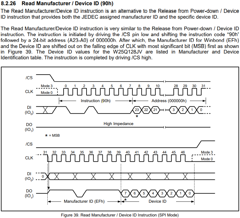
Looking up the [W25Q128 Data Sheet](https://www.winbond.com/resource-files/w25q128jv_dtr revc 03272018 plus.pdf), we can see that the instructions for querying manufacturer and device ID are as follows0x90
Instructions are described in the following figure

The code is as follows
log.info(PROJECT .. ".chipID", string.toHex(transfer(CS, spiID, string.char(0x90, 0, 0, 0), 4, 2)))
The log is as follows
I/user.spi.chipID EF17 4
In the return value 0xEF17, EF is the manufacturer Winbond Serial Flash, and 17 is the modelW25Q128JV
Erase specified address sector#
Looking up [W25Q128 Data Sheet](https://www.winbond.com/resource-files/w25q128jv_dtr REVVC 03272018 PLUS. pdf), we can see that the instruction to erase the specified address sector is0x20
A write enable instruction needs to be executed before an erase instruction can be executed0x06
Erase 4K-bytes size sector starting at address 0x01
The code is as follows
transfer(CS, spiID, string.char(0x06), 1, 0)
sys.wait(100)
transfer(CS, spiID, string.char(0x20, 0x00, 0x00, 0x01), 4, 0)
-- Erasing takes some time
sys.wait(1000)
Read and write SPI FLASH#
Looking up the [W25Q128 Data Sheet](https://www.winbond.com/resource-files/w25q128jv_dtr revc 03272018 plus.pdf), we can see that the instruction written on the page is0x 02, the maximum amount of data written at a time is 256 bytes, and the instruction for reading data is0x03
A write enable instruction needs to be executed before an erase instruction can be executed0x06
The code is as follows
transfer(CS, spiID, string.char(0x06), 1, 0)
sys.wait(100)
transfer(CS, spiID, string.char(0x02, 0x00, 0x00, 0x01) .. PROJECT, 4 + string.len(PROJECT), 0)
sys.wait(100)
local readRes = transfer(CS, spiID, string.char(0x03, 0x00, 0x00, 0x01), 4, string.len(PROJECT))
log.info(PROJECT .. ".readRes", readRes)
The log is as follows
I/user.spi.readRes spi
Looking at the log, the data read out is consistent with the data we wrote.
Disable write enable and turn off the corresponding SPI channel and CS GPIO#
Looking up the [W25Q128 Data Sheet](https://www.winbond.com/resource-files/w25q128jv_dtr revc 03272018 plus.pdf), it can be seen that the instruction to disable write enable is0x04
The code is as follows
transfer(CS, spiID, string.char(0x04), 1, 0)
gpio.close(CS_GPIO)
spi.close(spiID)
Abstraction for a SPI device and then read and write#
Abstract SPi Peripherals#
Abstract SPI channel 0 SPI FLASH,24MHz CLK, half duplex mode
The code is as follows
local spiID, CS_GPIO = 0, 20
-- The last mode parameter, 0, represents half-duplex mode.
local spiFlash = spi.deviceSetup(spiID, CS_GPIO, 0, 0, 8, 24 * 1000 * 1000, spi.MSB, 1, 0)
Manufacturers and devices that read SPI FLASH ID#
Looking up the [W25Q128 Data Sheet](https://www.winbond.com/resource-files/w25q128jv_dtr revc 03272018 plus.pdf), we can see that the instructions for querying manufacturer and device ID are as follows0x90
Instructions are described in the following figure

The code is as follows
log.info(PROJECT .. ".chipID", string.toHex(spiFlash:transfer(string.char(0x90, 0, 0, 0), 4, 2)))
The log is as follows
I/user.spi.chipID EF17 4
In the return value 0xEF17, EF is the manufacturer Winbond Serial Flash, and 17 is the modelW25Q128JV
Erase specified address sector#
Looking up [W25Q128 Data Sheet](https://www.winbond.com/resource-files/w25q128jv_dtr REVVC 03272018 PLUS. pdf), we can see that the instruction to erase the specified address sector is0x20
A write enable instruction needs to be executed before an erase instruction can be executed0x06
Erase 4K-bytes size sector starting at address 0x01
The code is as follows
spiFlash:send(string.char(0x06))
sys.wait(100)
spiFlash:send(string.char(0x20, 0x00, 0x00, 0x01))
-- Erasing takes some time
sys.wait(1000)
Read and write SPI FLASH#
Looking up the [W25Q128 Data Sheet](https://www.winbond.com/resource-files/w25q128jv_dtr revc 03272018 plus.pdf), we can see that the instruction written on the page is0x 02, the maximum amount of data written at a time is 256 bytes, and the instruction for reading data is0x03
A write enable instruction needs to be executed before an erase instruction can be executed0x06
The code is as follows
spiFlash:send(string.char(0x06))
sys.wait(100)
spiFlash:send(string.char(0x02, 0x00, 0x00, 0x01) .. PROJECT)
sys.wait(100)
local readRes = spiFlash:transfer(string.char(0x03, 0x00, 0x00, 0x01), 4, string.len(PROJECT))
log.info(PROJECT .. ".readRes", readRes)
The log is as follows
I/user.spi.readRes spi
Looking at the log, the data read out is consistent with the data we wrote.
Disable write enable and shut down the corresponding SPI channel#
Looking up the [W25Q128 Data Sheet](https://www.winbond.com/resource-files/w25q128jv_dtr revc 03272018 plus.pdf), it can be seen that the instruction to disable write enable is0x04
The code is as follows
spiFlash:send(string.char(0x04))
log.info(PROJECT .. ".device_close", spiFlash:close())
The log is as follows
I/user.spi.device_close true
Full Code#
PROJECT = "spi"
VERSION = "1.0.0"
sys = require("sys")

function transfer(CS, spiID, data, sendLen, recvLen)
    CS(0)
    local res = spi.transfer(spiID, data, sendLen, recvLen)
    CS(1)
    return res
end

local function test()
    local spiID, CS_GPIO = 0, 20
    local setupRes = spi.setup(spiID, 255, 0, 0, 8, 10 * 1000 * 1000, spi.MSB, 1, 0)
    if setupRes ~= 0 then
        log.error(PROJECT .. ".setup", "ERROR")
        return
    end
    local CS = gpio.setup(CS_GPIO, 0)
    log.info(PROJECT .. ".chipID", string.toHex(transfer(CS, spiID, string.char(0x90, 0, 0, 0), 4, 2)))
    transfer(CS, spiID, string.char(0x06), 1, 0)
    sys.wait(100)
    transfer(CS, spiID, string.char(0x20, 0x00, 0x00, 0x01), 4, 0)
    sys.wait(1000)
    transfer(CS, spiID, string.char(0x06), 1, 0)
    sys.wait(100)
    transfer(CS, spiID, string.char(0x02, 0x00, 0x00, 0x01) .. PROJECT, 4 + string.len(PROJECT), 0)
    sys.wait(100)
    local readRes = transfer(CS, spiID, string.char(0x03, 0x00, 0x00, 0x01), 4, string.len(PROJECT))
    log.info(PROJECT .. ".readRes", readRes)
    transfer(CS, spiID, string.char(0x04), 1, 0)
    gpio.close(CS_GPIO)
    spi.close(spiID)
    local spiFlash = spi.deviceSetup(spiID, CS_GPIO, 0, 0, 8, 10 * 1000 * 1000, spi.MSB, 1, 0)
    log.info(PROJECT .. ".chipID", string.toHex(spiFlash:transfer(string.char(0x90, 0, 0, 0), 4, 2)))
    spiFlash:send(string.char(0x06))
    sys.wait(100)
    spiFlash:send(string.char(0x20, 0x00, 0x00, 0x01))
    sys.wait(1000)
    spiFlash:send(string.char(0x06))
    sys.wait(100)
    spiFlash:send(string.char(0x02, 0x00, 0x00, 0x01) .. PROJECT)
    sys.wait(100)
    local readRes = spiFlash:transfer(string.char(0x03, 0x00, 0x00, 0x01), 4, string.len(PROJECT))
    log.info(PROJECT .. ".readRes", readRes)
    spiFlash:send(string.char(0x04))
    log.info(PROJECT .. ".device_close", spiFlash:close())
end

sys.taskInit(test)

sys.run()