Air105 Chip#
1. Overview#
1.1 Product overview#
Hezhou Air105 is a QFN88 MCU with a size of 10mm x 10mm. It not only provides basic peripherals such as UART/GPIO/I2C/ADC/SPI, but also provides advanced peripheral interfaces such as DAC/USB/DCMI/HSPI/LCDI/KCU. It has built-in charging function, supports 5V/3.3V power supply, and comes with 5v to 3.3V LDO,4M byte Flash and 640K byte RAM. Internal flash start address 0x01001000
1.2 Electrical Performance#
Limit parameter
**Parameter ** |
Description |
Range |
** Unit** |
|---|---|---|---|
Iddpd |
Shutdown current |
- |
nA |
Tamb |
Working temperature |
-40~+85 |
℃ |
Tstg |
Storage temperature |
-40~+125 |
℃ |
Ground |
ground |
-0.3~0.3 |
V |
Voh |
Digital output high level |
VDD -0.3 ~ VDD+0.3 |
V |
Vol |
Digital output low level |
<0.4 |
V |
Ioh |
pull current(PA2/3/4/5, PC6/7/8/9) |
27(@3V) |
mA |
pull current (other IO) |
16(@3V) |
mA |
|
Iol |
Irrigation current(PA2/3/4/5, PC6/7/8/9) |
27(@0.5V) |
mA |
Sprinkling current (other IO) |
16(@0.5V) |
mA |
|
Vih |
Digital input high level |
≥0.7×VDD |
V |
ViL |
Digital input low level |
≤0.3×VDD |
V |
Electrical characteristics
**Parameter ** |
** Condition (-40°C to 85°C)** |
Value |
** Unit** |
|
|---|---|---|---|---|
**Minimum ** |
** Maximum** |
|||
VCC |
3.6 |
5.5 |
V |
|
CHARGE_VCC |
4.7 |
5.5 |
V |
|
AVD33 |
2.7 |
3.6 |
V |
|
VDD33 |
2.7 |
3.6 |
V |
|
VBAT33 |
2 |
3.6 |
V |
|
Vol |
VDD=3.3V |
- |
0.4 |
V |
Voh |
VDD=3.3V |
V |
||
VIH |
VDD=3.3V |
0.7×VDD |
V |
|
VIL |
VDD=3.3V |
0.3×VDD |
V |
Safety-related features
**Sensor ** |
Description |
Range |
** Unit** |
|---|---|---|---|
Voltage Sensor |
Main Supply Voltage High Voltage Detection Range |
4.0±0.1 |
V |
Main power supply voltage low voltage detection range |
2.8±0.1 |
V |
|
Battery voltage high voltage detection range |
4.0±0.1 |
V |
|
Battery voltage low voltage detection range |
1.9±0.1 |
V |
|
Clock Frequency Sensor |
12M Clock Frequency Detection Range |
12±50% |
MHz |
32K Clock Frequency Detection Range |
32±50% |
KHz |
1.3 Pin Definition#

The following figure shows the pin definition of Air105, which supports up to 54 GPIO, and each IO is multiplexed with peripherals. Each GPIO can be configured as an input, output, interrupt mode, when as an output, each IO output value can be individually configured. The IO supports strong push-pull output/open-drain output mode.
Pin Details ( Default state after all general I/O reset is pull-up, resistance value 51KΩ)
**Number ** |
Name |
Type |
Reuse Function |
Pull Up and Down Capability |
** Remarks** |
|---|---|---|---|---|---|
1 |
CVCC |
P |
NC |
||
2 |
VDD33 |
P |
Minimum voltage 2.7V, maximum voltage 3.6V |
||
3 |
VCC |
P |
The minimum input voltage is 3.6V, and the maximum voltage is 5.5V |
||
4 |
VDD33_OUT |
P |
Chip 3.3V Output |
The output capacity of the chip is about 400mA. When the peripheral load uses the chip’s 3.3V, pay attention to the maximum current |
|
5 |
NC |
NC |
|||
6 |
PA7 |
I/O |
GPIO7/SPI1_CSN |
UP |
|
7 |
PA6 |
I/O |
GPIO6/SPI1_SCK |
UP |
|
8 |
PB2 |
I/O |
GPIO18/SPI2_SCK |
UP |
|
9 |
PB3 |
I/O |
GPIO19/SPI2_CSN |
UP |
|
10 |
PB4 |
I/O |
GPIO20/SPI2_MOSI/UART2_CTS |
UP |
|
11 |
PB5 |
I/O |
GPIO21/SPI2_MISO/UART2_RTS |
UP |
|
12 |
PE6 |
I/O |
GPIO70//UART3_CTS/I2C0_SCL |
UP |
|
13 |
PE7 |
I/O |
GPIO71/UART3_RTS/I2C0_SDA |
UP |
|
14 |
PE8 |
I/O |
GPIO72/UART3_RX |
UP |
|
15 |
PE9 |
I/O |
GPIO73/UART3_TX |
UP |
|
16 |
PE10 |
I/O |
GPIO74/UART3_CTS |
UP |
|
17 |
PE11 |
I/O |
GPIO75/UART3_RTS |
UP |
|
18 |
PA0 |
I/O |
UART0_RX |
Serial download |
fixed |
19 |
PA1 |
I/O |
UART0_TX |
Fixed |
|
20 |
PA2 |
I/O |
GPIO2/UART0_CTS/PWM2 |
UP |
|
21 |
PA3 |
I/O |
GPIO3UART0_RTS/PWM3 |
UP |
|
22 |
PB0 |
I/O |
GPIO16/PWM0/XTAL32K |
UP |
|
23 |
PB1 |
I/O |
GPIO17/PWM1/CLK_24M |
UP/Configurable output 24M |
|
24 |
CHARGE_VBAT |
P |
CHARGE Power output, connected to the battery |
can charge 3.7V lithium battery, the maximum charging current 200mA |
|
25 |
CHARGE_VCC |
P |
CHARGE Power input |
minimum input voltage is 4.7V, maximum voltage is 5.4V |
|
26 |
PD1 |
I/O |
GPIO49/DCMIS_DATA0 |
UP |
|
27 |
PD2 |
I/O |
GPIO50/DCMIS_DATA1 |
UP |
|
28 |
PD3 |
I/O |
GPIO51/DCMIS_DATA2 |
UP |
|
29 |
PD8 |
I/O |
GPIO56/DCMIS_DATA3 |
UP |
|
30 |
PD9 |
I/O |
GPIO57/DCMIS_DATA4 |
UP |
|
31 |
PD10 |
I/O |
GPIO58/KeyBoard7/DCMIS_DATA5 |
UP |
|
32 |
PD11 |
I/O |
GPIO59/KeyBoard8/DCMIS_DATA6 |
UP |
|
33 |
PE0 |
I/O |
GPIO64/KeyBoard4/DCMIS_DATA7 |
UP |
|
34 |
PD6 |
I/O |
GPIO54/UART1_CTS/DCMIS_DATA8 |
UP |
|
35 |
PD7 |
I/O |
GPIO55/UART1_RTS/DCMIS_DATA9 |
UP |
|
36 |
PC6 |
I/O |
GPIO38/PWM4/DCMIS_DATA10 |
UP |
|
37 |
PC7 |
I/O |
GPIO39/PWM5/DCMIS_DATA11 |
UP |
|
38 |
PC8 |
I/O |
GPIO40/PWM6/DCMIS_DATA12 |
UP |
|
39 |
PC9 |
I/O |
GPIO41/PWM7/DCMIS_DATA13 |
UP |
|
40 |
PE1 |
I/O |
GPIO65/KeyBoard5/DCMIS_VSYNC |
UP |
|
41 |
PE2 |
I/O |
GPIO66/KeyBoard6/DCMIS_HSYNC |
UP |
|
42 |
PE3 |
I/O |
GPIO67/DCMIS_PIX_CLK |
UP |
|
43 |
PB12 |
I/O |
GPIO28/SPI0_CLK |
UP |
|
44 |
VSS |
GND |
Chip ground |
||
45 |
PB13 |
I/O |
GPIO29/SPI0_CSN |
UP |
|
46 |
PB14 |
I/O |
GPIO30/SPI0_MOSI/UART1_CTS |
UP |
|
47 |
PB15 |
I/O |
GPIO31/SPI0_MISO/UART1_RTS |
UP |
|
48 |
PC12 |
I/O |
GPIO44/SPI5_MISO |
UP |
|
49 |
PC13 |
I/O |
GPIO45/SPI5_MOSI |
UP |
|
50 |
PC14 |
I/O |
GPIO46/SPI5_CSN |
UP |
|
51 |
PC15 |
I/O |
GPIO47/SPI5_CLK |
UP |
|
52 |
VDD33 |
P |
|||
53 |
PD13 |
I/O |
GPIO61/UART2_TX/KeyBoard1 |
UP |
|
54 |
PD12 |
I/O |
GPIO60/UART2_RX/KeyBoard0 |
UP |
|
55 |
PD15 |
I/O |
GPIO63/UART2_RTS/KeyBoard3 |
UP |
|
56 |
PD14 |
I/O |
GPIO62/UART2_CTS/KeyBoard2 |
UP |
|
57 |
NC |
NC |
|||
58 |
NC |
NC |
|||
59 |
NC |
NC |
|||
60 |
NC |
NC |
|||
61 |
REFP |
O |
1uF capacitor to ground |
||
62 |
PC5 |
I/O |
GPIO37/ADC_IN6/CLK_27P12 |
Configurable output 27.12M |
|
63 |
PC4 |
I/O |
GPIO36/ADC_IN5/XTAL32K |
UP |
|
64 |
PC3 |
I/O |
GPIO35/ADC_IN4/UART1_RTS |
UP |
|
65 |
PC1 |
I/O |
GPIO33/ADC_IN2/DAC/UART1_TX |
Digital Audio to Analog Audio Interface |
|
66 |
PC0 |
I/O |
GPIO32/ADC_IN1/UART1_RX |
UP |
|
67 |
VDD25 |
O |
1uF ground capacitance |
||
68 |
DN |
I |
Pay attention to maintain differential routing, and do a good job of 90 Ohm control of impedance. |
||
69 |
DP |
O |
|||
70 |
VBUS |
I |
Series 100Ω electrical impedance surge |
||
71 |
VDD33 |
P |
Minimum voltage 2.7V, maximum voltage 3.6V |
||
72 |
XO12M |
0 |
XTAL 12MHz Output |
The chip supports an internal 12MHz oscillator and an external 12MHz crystal. For chip-to-chip interface when using an external 12MHz crystal, please refer to the clock circuit below. |
|
73 |
XI12M |
1 |
XTAL 12MHz Input |
Ibid. |
|
74 |
VDD12 |
O |
1uF ground capacitance |
||
75 |
AVD33 |
P |
Minimum voltage 2.7V, maximum voltage 3.6V |
||
76 |
XI32 |
I |
XTAL 32KHz Input |
The chip supports internal or external 32KHz output, using external 32KHz circuit can refer to the following clock circuit |
|
77 |
XO32 |
O |
XTAL 32KHz Output |
Ibid. |
|
78 |
NC |
NC |
|||
79 |
NC |
NC |
|||
80 |
NC |
NC |
|||
81 |
NC |
NC |
|||
82 |
NC |
NC |
|||
83 |
NC |
NC |
|||
84 |
VBAT33 |
P |
button battery |
||
85 |
PA5 |
I/O |
GPIO5/CLK_24M |
Configurable output 24M |
|
86 |
PA8 |
I/O |
GPIO8/SPI1_MOSI |
When multiplexing is IO, the IC card power must be turned on first, and the high level of the output signal is the IC card output level |
|
87 |
PA9 |
I/O |
GPIO9/SPI1_MISO |
Ibid. |
|
88 |
PA10 |
I/O |
GPIO10 |
Ibid. |
Note: I, on behalf of the input; O, on behalf of the output; P, on behalf of the power supply
Note: PWM6/7 is not available under LuatOS firmware
2. peripheral circuit design#
2.1 power supply circuit#
The chip has 2 power supply modes:
Internal LDO, input power supply through VCC pin, internal conversion output 3.3V, power supply source is 3.6~5.5V USB or lithium battery. Internal LDO output capacity is limited, if you need to drive high-power peripherals, please add additional LDO or DC2DC.
3.3V Direct supply, the power supply range is 3.2V ~ 3.4V, which is directly supplied to the VCC33 pin of the chip.
2.2 on/off circuit#
The on-off circuit realizes the on-off function of the chip by controlling the internal 5V to 3.3V LDO enable/close. When using the CHARGE_VBAT power supply and the on-off function, it should be noted that the VBAT33 pin is in place. When the chip is not powered on, the internal LDO enable is POWER_KEY pulled up for 150ms. By POWER_KEY the power-on circuit, it should be noted that the POWER_KEY key is usually low and pressed to pull up. When the CHARGE_VCC is powered (voltage range 4.7V ~ 5.4V), the internal LDO can directly output 3.3V and cannot be shut down. You can refer to the two power-on power supply methods in the following figure.
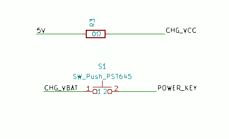
The shutdown function can turn off the internal LDO output by POWER_KEY pulling up 7S to achieve the purpose of shutdown.
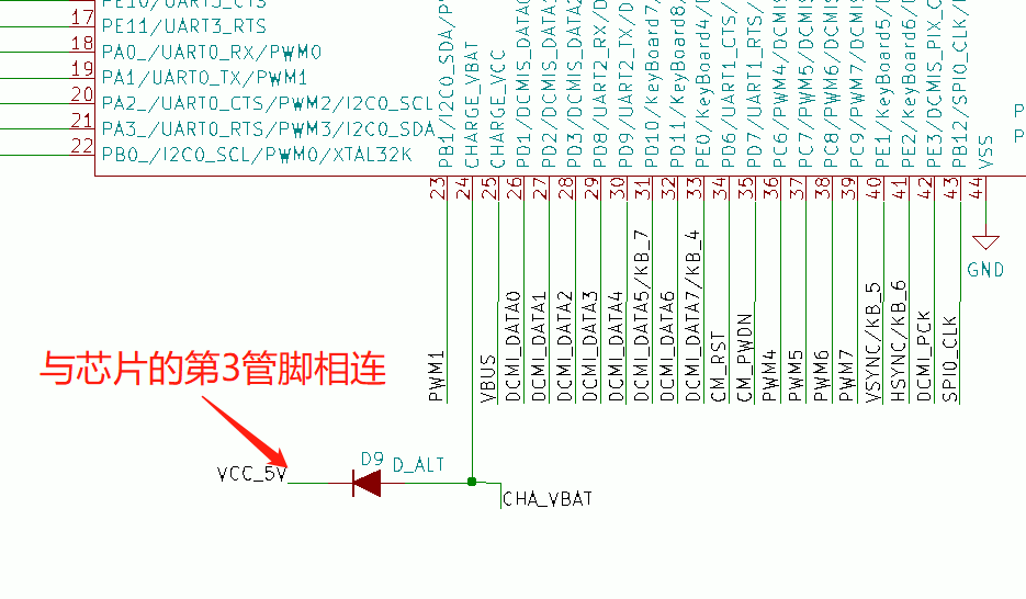
2.3 Charging module circuit#
Air105 The chip supports the battery charging function, can charge 3.7V lithium battery, supports a maximum charging current of 200mA, and the battery is fully charged at a voltage of 4.15±0.05V. After the battery is fully charged, the battery will be recharged after the voltage drops to 4.05V. When the battery supplies power to the module, it is recommended to add a diode switching circuit.
2.4 LDO#
Air105 When the VCC input voltage of the chip is 4-5.5V, the maximum driving capability of the internal LD0 is 400mA, so when there are many peripheral loads, some external LDO circuits should be considered.
2.5 clock circuit#
The chip supports an internal 12MHz oscillator and an external 12MHz crystal. The accuracy of the internally integrated 12MHz crystal is 2%. After PLL frequency multiplication, it provides input to the system. The PLL clock frequency after frequency multiplication can be configured by software, and its frequency can be configured:108MHz、 120MHz、132MHz、144MHz、156MHz、168MHz、180MHz、192MHz、204MHz。
When selecting an external 12MHz crystal oscillator, crystals with different temperature levels, stability and load capacitance values are selected according to actual product requirements. The load capacitance connected to both ends of the crystal needs to be adjusted according to the crystal of different manufacturers and the frequency offset.
The crystal is placed as close to the chip as possible, the trace is as short as possible, and it is far away from the interference source. The clock is isolated from many holes. The layers below the clock prohibit other traces from passing through to prevent interference with the clock source.
The entire safety zone of the chip works based on the internal 32KHz. RTC works based on the internal OSC 32K by default. The software can switch to use the external XTAL 32K to work and support the internal or external 32KHz output.
2.6 I2C Circuit#
I2C(Inter-chip) bus interface connects the microcontroller and the serial I2C bus. It provides multi-master functionality, controlling all I2C bus-specific timing, protocol, arbitration, and timing. Supports both standard and fast modes. Depending on the needs of a particular device, DMA may be used to reduce the burden on the CPU.
In terms of circuit, 4.7K pull-up should be added at I2C interface 3.3V。
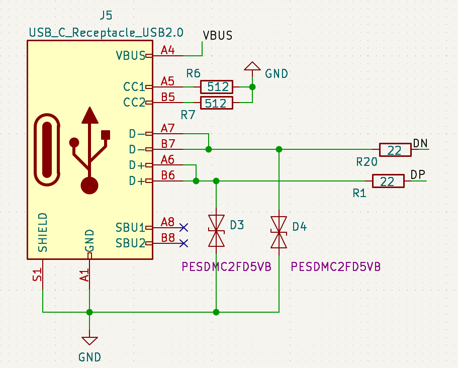
2.7 USB Circuit#
Air105 When connecting USB, attention should be paid to DN and DP to ensure impedance control of 90 Ohm and differential routing. A resistor of 100Ω should be connected in series from VBUS pin to chip for surge resistance, and a resistor of 22 ohms (or other resistors such as 33 ohms) should be connected in series on the signal line to prevent signal reflection. Please refer to the following schematic diagram.
3. Reference Circuit Design#
Air105 The power supply voltage of the chip is 5V, the normal working power supply range is 4.0V ~ 5.5V, and the maximum driving capacity of the internal LDO is 400mA. Pay attention to the peripheral load to avoid exceeding the maximum driving capacity. Each power input pin of the chip should be placed with a corresponding filter capacitor, and a capacitor of 1uF to ground should be added to the three pins 61, 67 and 74.
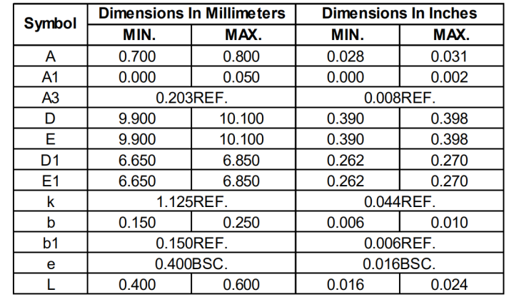
4. Package Size#
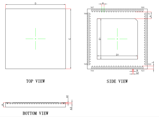
parameter comparison table